Aiming to Become a World-Leading Semiconductor Materials Supplier
with Robust Overall Capabilities

Focused on Lean Manufacturing for Superior Quality and Industry Advancement

Dedicated to Delivering Excellent Total Solutions for Customers Worldwide

Leading with Innovation and Embracing
Responsibility to Build a Sustainable Future

Building a World-Leading R&D and Manufacturing Hub
for Semiconductors and Silicon Wafers

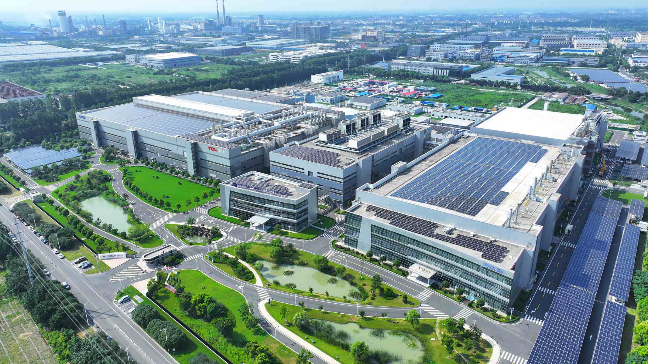
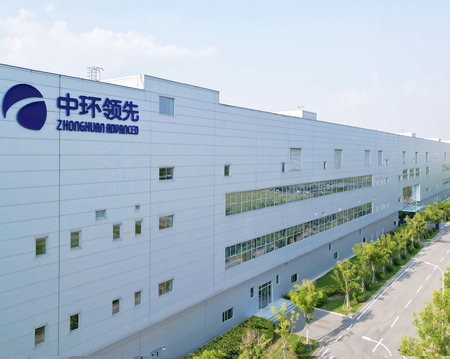
Zhonghuan Advanced specializes in the R&D and manufacturing of semiconductor materials and products for related industries. We are committed to providing excellent total solutions for customers worldwide. Our product line includes polished, epitaxial, annealed, chemically etched, and SOI wafers, ranging from 4 inches to 12 inches. By utilizing superior resources in Yixing, Xuzhou, Tianjin, and Hohhot, we have established a comprehensive industrial presence across China through our coordinated efforts. In addition, we have set up sales centers in other countries and regions such as Singapore, Japan, South Korea, Europe, and the Taiwan region to drive our global expansion.

Building a World-Leading R&D and Manufacturing Hub<br> for Semiconductors and Silicon Wafers
1300 K slices per month


300mm Wafers Planned Capacity

e1(1724206837011).png
e2(1724206845626).png
e3(1724206859978).png
1100 K slices per month


200mm Wafers Planned Capacity

d1(1724206692908).png
d2.png
d3.png
d4.png
d5.png
1100 K slices per month


≤150mm Wafers Planned Capacity

c1(1724206444647).png
c2.png
c3.png

No.1


Revenue and Shipment Area in China

b1.png
b2.png
b3.png
Total Solutions

One-Stop Customized Services
for Silicon-Based Products

Polished Wafers


Polished wafers are produced from FZ,CZ,or MCZ silicon ingots. These wafers achieve near-perfect surfaces that meet the highest standards for flatness and surface quality through cutting, lapping, polishing, and other processes. Depending on the dopant concentration, polished wafers are classified as either lightly doped or heavily doped.

Epitaxial Wafers


Epitaxial wafers are polished wafers with one or more additional layers through epitaxy. These layers have specific dopant types, resistivity, thickness, and lattice structures.

SOI Wafers


SOI (silicon-on-insulator) wafers feature an oxide insulator buried layer between the top silicon layer and the supporting substrate. This structure can be used to produce high-performance, low-power, and highly integrated chips.

Argon-Annealed Wafers


Argon-annealed wafers are polished wafers that have been annealed (treated with heat) in an argon environment to produce a clean surface layer. The annealing process helps to remove impurities and eliminate surface defects, thereby enhancing device performance.

SiC Epitaxial Wafers


SiC (silicon carbide) epitaxial wafers are silicon carbide wafers with a monocrystalline thin film grown on the substrate. This film meets specific requirements and aligns with the orientation of the substrate.

Silicon-based GaN Epitaxial Wafers


Silicon-based GaN (gallium nitride) epitaxial wafers are characterized by a wide band gap, high thermal conductivity, and excellent resistance to heat, radiation, and acid/alkali environments. They also exhibit great strength and hardness.

Other Products


Lapped silicon wafers can be transformed into polished epitaxial wafers through polishing and other precision processes. Etched silicon wafers are produced through mixed acid etching, which removes the stress-damaged layer from the surface to maintain high-quality monocrystalline characteristics.

Industrial Layout


Yixing


IC-Grade Semiconductor Wafer R&D and Manufacturing Center

Yixing Fab specializes in developing and manufacturing a full range of products from 8 to 12 inches. The factory that produces 12-inch products utilizes a dual "power + IC" strategy and aims to produce 700K slices per month. The factory for 8-inch products focuses on logic and power chips.

View Details

Xuzhou


IC-Grade Semiconductor Wafer R&D and Manufacturing Center

Xuzhou Fab is dedicated to the R&D and manufacturing of 12-inch wafers for integrated circuits, primarily for logic and memory chips. It is certified by top international customers and delivers an exceptional average defect-free crystal rate. The facility plans to produce 600K slices per month.

View Details

Tianjin


Power Products R&D and Manufacturing Center

Aiming to become the largest specialized power semiconductor materials production base in Northern China,Tianjin Fab implements smart production lines for wafers with diameters of 8 inches and below. It also leverages the advantages of both the floating zone (FZ) and Czochralski (CZ) processes to deliver premium quality.

View Details

Hohhot


Crystals R&D and Manufacturing Center

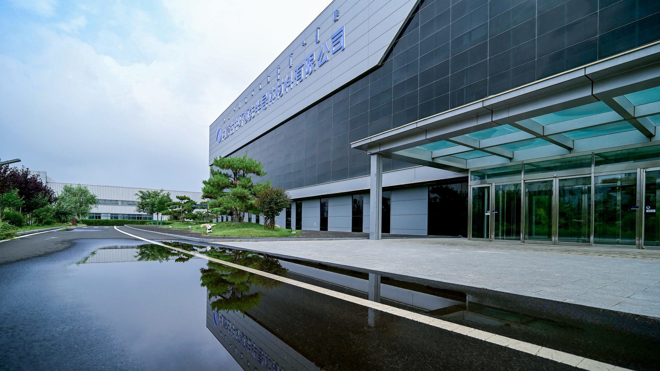
Hohhot Fab will be developed into a leading R&D and manufacturing hub for CZ crystals with optimal economies of scale. It will extend the semiconductor ingot industry chain through resource optimization and industry coordination.

View Details

Yixing
Xuzhou
Tianjin
Hohhot

Yixing

Xuzhou

Tianjin

Hohhot