Becoming a World-Leading Semiconductor Materials Company
with Robust Overall Capabilities

Company Profile

Zhonghuan Advanced focuses on the R&D and manufacturing of semiconductor materials and products for related industries. Driven by innovation, we provide excellent total solutions worldwide and aim to become a world-leading supplier of semiconductor materials.
Company Profile

*Data as of December 31, 2025

5.761
CNY 5.761 billion

Annual revenue

34.4
CNY 34.4 billion

Total assets

1223
1223 MSI

Shipment area

3787
About 3787

Employees

Marketing Cluster

Picture Name

Singapore

South Korea

Japan

Europe

United States

China

Jiangsu

Tianjin

Beijing

Shanghai

Shenzhen

Taiwan

Wuhan

Hefei

Industrial Layout

Yixing Factory

Xuzhou Factory

Tianjin Factory

Hohhot Factory

Yixing

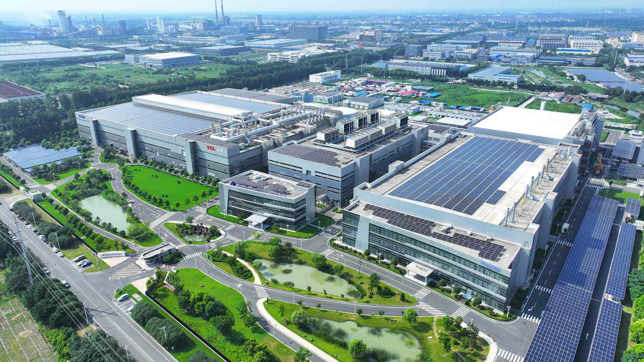
IC-Grade Semiconductor Wafer R&D and Manufacturing Center

Yixing Fab specializes in developing and manufacturing a full range of products from 8 to 12 inches. The factory that produces 12-inch products utilizes a dual "power + IC" strategy and aims to produce 700K slices per month. The factory for 8-inch products focuses on logic and power chips.
IC-Grade Semiconductor Wafer R&D and Manufacturing Center
Xuzhou

IC-Grade Semiconductor Wafer R&D and Manufacturing Center

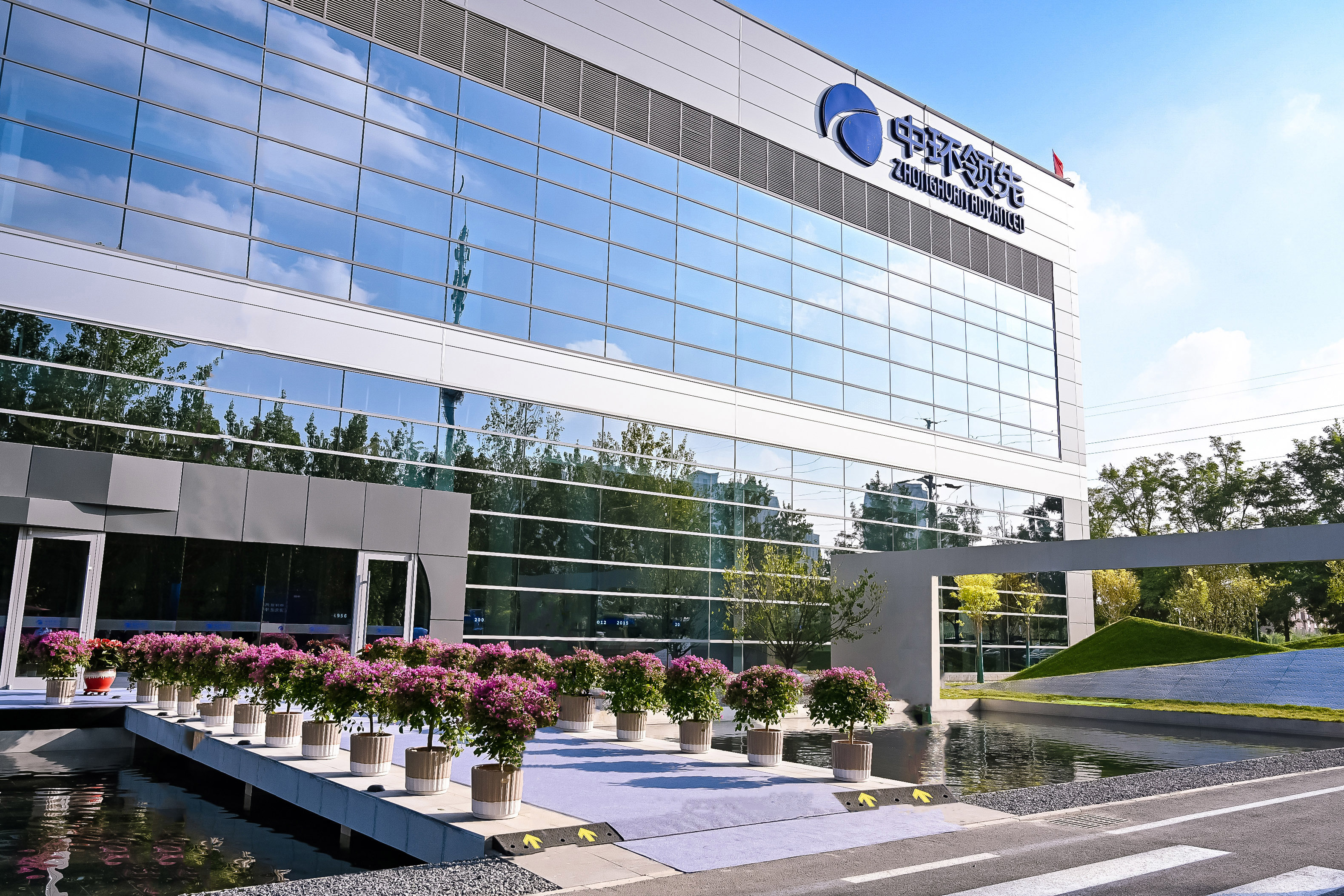
Xuzhou Fab is dedicated to the R&D and manufacturing of 12-inch wafers for integrated circuits, primarily for logic and memory chips. It is certified by top international customers and delivers an exceptional average defect-free crystal rate. The facility plans to produce 600K slices per month.
IC-Grade Semiconductor Wafer R&D and Manufacturing Center
Tianjin

Power Products R&D and Manufacturing Center
Aiming to become the largest specialized power semiconductor materials production base in Northern China,Tianjin Fab implements smart production lines for wafers with diameters of 8 inches and below. It also leverages the advantages of both the floating zone (FZ) and Czochralski (CZ) processes to deliver premium quality.
Power Products R&D and Manufacturing Center
Hohhot

Crystals R&D and Manufacturing Center

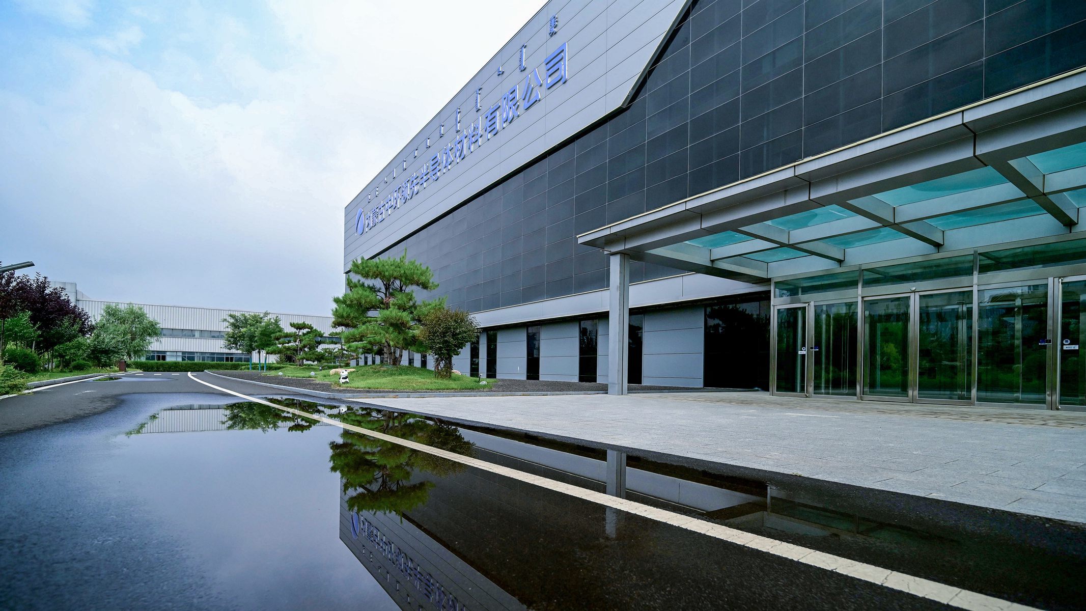
Hohhot Fab will be developed into a leading R&D and manufacturing hub for CZ crystals with optimal economies of scale. It will extend the semiconductor ingot industry chain through resource optimization and industry coordination.
Crystals R&D and Manufacturing Center

Our History

1956
R&D of germanium crystals was initiated
1958
Tianjin Semiconductor Material Factory was founded as one of China’s earliest enterprises engaged in semiconductor material production
1969
R&D of silicon crystals was initiated
1973
R&D of Φ1.5–2 inch epitaxial wafers was initiated
1978
The production of zone‑melted monocrystalline silicon was launched, and mass production of Φ2‑inch zone‑melted silicon wafers was achieved
1981
Tianjin Semiconductor Material Factory became one of China’s earliest manufacturers of solar monocrystalline silicon, producing Φ2–3 inch silicon wafers for photovoltaic cells
1985
Guided by national strategies, zone melting furnaces were introduced during the 6th Five‑Year Plan, expanding business scope from zone‑melted monocrystalline silicon to power semiconductors. Based on CZ silicon wafer manufacturing, the industrial chain was further extended to polished wafers and epitaxial wafers
1989
82 mm zone-melted wafers were produced for 4500 V, 1500 A high-voltage DC devices used in State Grid electric locomotives
1997
The CFZ project was launched, and its products are applied to semiconductor material devices
1999
The pulling of Φ4-inch zone-melted monocrystalline silicon was realized, breaking the international monopoly
2000
Tianjin HuanOu Semiconductor Material & Technology Co., Ltd. was established
2026
The large-diameter silicon wafer project in Shenzhen was officially launched
2023
Completed our strategic restructuring,
and officially launched our Xuzhou Fab.
2022
Established a semiconductor materials research institute and launched a CNAS lab.
2020
Commenced mass production of 300mm polished wafers for integrated circuits.
2019
Achieved a significant breakthrough in developing 300mm COP-free ingots.
2017
Launched the production base for 200mm-300mm silicon wafers for integrated circuits.
2015
Launched the R&D and manufacturing center for CZ ingots in Hohhot.
2012
Commenced mass production of 200mm CZ heavily doped polished silicon wafers.
2011
Successfully produced the first 200mm FZ monocrystalline silicon wafer.
2008
Commenced production of 150mm polished silicon wafers for power devices.
2003
Transitioned from inner diameter cutting to multi-wire saw cutting for silicon wafers.
2002
Successfully produced the first 150mm FZ monocrystalline silicon wafer.